
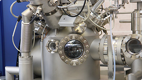

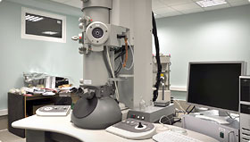

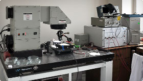
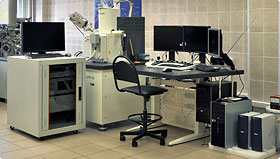

3D-probe system «GPI-Cryo-SEM»
Types of analysis by high resolution scanning probe microscopy methods:
- Image acquisition mode tunneling microscope.
- Measuring the thickness of thin layers of films and heterostructures in the range of 1 - 100 nm.
- Measuring of electric parameters of micro- and nanoelectronics.
- Nanolithography
- Spectroscopic studies of micro-and nano-electronics structures
 |  |
|
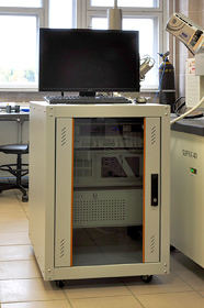
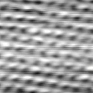
Pyrolytic graphite surface. The crystal lattice and the individual atoms of carbon are visible. Raster · 17.8 17.8 nm 3D-nano-probe system «GPI-Cryo-SEM» - Supra 40 SEM vacuum system-based scanning tunneling microscope |

